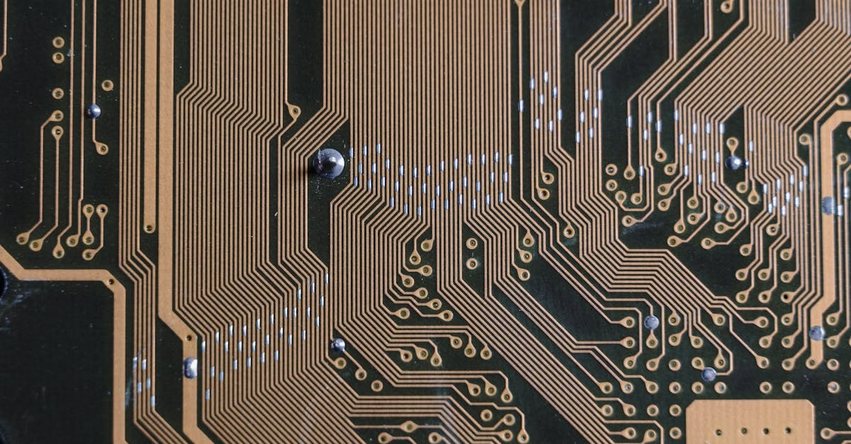
Printed circuit boards (PCBs) are the backbone of modern electronics, connecting and supporting electronic components in virtually every device we use. The design and fabrication of these intricate structures have evolved significantly over the decades, driven by increasing circuit complexity, miniaturization, and performance demands. One technique that played a crucial role in the development of high-density PCBs, particularly in the era of through-hole technology, was the copper pullback technique. While less common in contemporary surface-mount-dominated designs, understanding the pullback technique provides valuable insight into the historical challenges of PCB fabrication and the evolution of design rules.
The Genesis of Copper Pullback: Addressing Manufacturing Imperfections
The pullback technique emerged as a solution to a specific set of manufacturing challenges prevalent in the era of through-hole technology. Early PCB manufacturing processes were less precise than they are today. Drilling holes for component leads and etching the copper traces were subject to greater tolerances and variations. One significant issue was the potential for annular ring breakout.
The annular ring is the copper area surrounding a drilled hole, providing the electrical connection between the component lead and the circuit trace. Ideally, the drilled hole should be perfectly centered within the annular ring. However, due to drilling inaccuracies, the hole could be offset, potentially breaking out of the annular ring. This breakout would result in a broken connection, rendering the board defective.
Copper pullback aimed to mitigate the risk of annular ring breakout. It involved intentionally increasing the width of the copper traces before they connected to the pad surrounding the drilled hole. This wider section of the trace, the “copper pullback,” effectively extended the annular ring, providing a larger target for the drill and increasing the tolerance for drilling inaccuracies. Even if the drill was slightly off-center, the connection was more likely to be maintained within the wider pullback area.
Why Pullback Was Necessary: A Multifaceted Approach to Reliability
The necessity of the pullback technique stemmed from a combination of factors related to the limitations of early PCB manufacturing processes and the reliability requirements of electronic devices.
- Drilling Inaccuracies: Drilling technology in the early days of PCB manufacturing was less precise than today’s CNC-controlled drilling machines. Drill bits were prone to wander, and maintaining consistent hole placement was a challenge. Copper pullback provided a buffer against these inaccuracies.
- Etching Variations: The etching process, which defines the copper traces, was also subject to variations. Over-etching could reduce the width of the traces, potentially compromising the connection at the pad. The wider pullback area provided additional copper, making the connection more robust even with some degree of over-etching.
- Component Lead Variations: Component leads themselves were not always perfectly uniform in diameter. Pullback accommodated slight variations in lead size, ensuring a secure connection even if the lead was slightly larger than the nominal hole size.
- Increased Reliability: Ultimately, the primary driver for using pullback was to improve the reliability of the finished PCB. By minimizing the risk of annular ring breakout, pullback reduced the likelihood of manufacturing defects and ensured a more robust and reliable electrical connection. This was particularly crucial in applications where failure could have significant consequences.
The Design and Implementation of Pullback:
Implementing pullback involved modifying the PCB layout during the design phase. Designers would manually increase the width of the traces leading to the pads, ensuring that the wider section extended sufficiently beyond the expected drill tolerance. This required careful consideration of the specific manufacturing capabilities and design rules.
The size and shape of the pullback area were typically defined in the design rules, taking into account factors such as the drill size, the pad size, and the manufacturing tolerances. These rules would dictate the minimum width of the pullback, the distance it should extend from the pad, and any other specific requirements.
The Decline of Copper Pullback: The Rise of Surface Mount Technology and Advanced Manufacturing
With the advent of surface mount technology (SMT) and advancements in PCB manufacturing processes, the need for pullback has significantly diminished. Several factors contributed to this decline:
- Surface Mount Technology: SMT components are soldered directly onto the surface of the PCB, eliminating the need for through-holes altogether. This inherently eliminates the issue of annular ring breakout, making pullback irrelevant.
- Improved Drilling Accuracy: Modern CNC-controlled drilling machines offer significantly improved drilling accuracy and precision. Hole placement is much more consistent, reducing the risk of breakout even without pullback.
- Advanced Etching Techniques: Etching processes have also improved, providing finer control over trace widths and reducing variations. This minimizes the risk of over-etching and ensures more consistent connections.
- Automated Design Tools: Modern PCB design software automates many aspects of the design process, including the application of design rules. While some design rules might still address specific manufacturing considerations, the manual implementation of pullback is no longer necessary.
Why Substrate PCBs Don’t Need Pullback:
Substrate PCBs, often used in advanced packaging and microelectronics, represent the cutting edge of PCB technology. These boards are characterized by extremely fine lines, small vias, and high component density. They rely heavily on SMT and advanced manufacturing techniques, making pullback completely unnecessary.
- Fine Line Technology: Substrate PCBs utilize extremely fine line technology, where trace widths are often in the micrometer range. Pullback, which involves widening traces, is incompatible with this level of miniaturization.
- Microvias: Substrate PCBs often employ microvias, which are very small vias (connections between layers) created using laser drilling or other advanced techniques. These microvias are significantly smaller than traditional through-holes, further reducing the concern for annular ring breakout.
- High-Density Packaging: Substrate PCBs are designed for high-density packaging, where space is at a premium. Pullback would consume valuable space and limit the density of components that can be placed on the board.
Conclusion:
The pullback technique, while largely a relic of the past, played a vital role in the evolution of PCB technology. It represents a clever solution to the manufacturing challenges of its time, improving the reliability of through-hole PCBs in an era of less precise fabrication processes. The advent of SMT and advancements in manufacturing have rendered pullback obsolete in most modern PCB designs, particularly in substrate PCBs. Understanding the historical context of pullback provides valuable insight into the challenges of PCB fabrication and the continuous drive for improved reliability and miniaturization in electronic design. While pullback may no longer be a standard practice, its legacy serves as a reminder of problem-solving techniques.