Full Schematic & Hierarchical Design Best Practices Guide
I. Introduction: Elevating Your Electronics Design with KiCAD SPICE Simulation
A. The Critical Role of Simulation in Modern Circuit Development
At IDEANT, we believe that circuit simulation has transcended its role as a mere convenience to become an indispensable phase in contemporary electronics design. This powerful capability empowers engineers to emulate electronic circuits through software, offering significant cost and time efficiencies. Simulation enables rigorous functionality checks without the immediate need for physical hardware prototypes, providing a virtual testbed where designs can be thoroughly vetted. It facilitates the precise assessment of parasitic element influences, allowing designers to understand how real-world imperfections might affect circuit performance. Furthermore, simulation supports the rapid evaluation of diverse circuit variants and the exploration of novel concepts with significantly reduced effort and risk compared to physical prototyping. This also provides a robust mechanism for cross-checking designs against automatically generated circuits, ensuring design integrity.
The benefits of simulation extend beyond mere technical validation. By minimizing research and development expenditure and accelerating time-to-market, simulation provides a significant strategic advantage for individuals and organizations. The ability to iterate quickly and test concepts virtually means that innovation can be pursued more aggressively and with lower financial risk. This transforms simulation into a critical business enabler, rather than solely an engineering task, fostering an environment of continuous improvement and competitive differentiation.
B. KiCAD and Ngspice: An Integrated Powerhouse for Circuit Analysis
Since version 5.0, KiCAD has seamlessly integrated ngspice, a robust open-source SPICE simulator, creating a powerful environment for circuit analysis. In this symbiotic relationship, KiCAD functions as an intuitive graphical user interface (GUI), acting as a “middleman” between the designer and the powerful ngspice engine. This integration allows users to design schematics and initiate simulations directly from the Schematic Editor, streamlining the workflow. ngspice offers broad compatibility with existing models from other popular SPICE variants, including LTspice, PSpice, and HSpice, enhancing its versatility. This unified environment significantly simplifies the design process by eliminating the need to learn disparate simulation user interfaces and simplifying the transfer of schematic sections for dedicated simulation.
The deep integration of simulation capabilities within KiCAD encourages designers to incorporate it frequently and iteratively throughout their workflow. When a crucial tool like simulation is easy to use and part of the main design environment, engineers are more inclined to adopt an “early and often” simulation mindset. This proactive approach enables the detection and rectification of design flaws at much earlier stages of development, compounding the cost and time savings. The result is a more agile and efficient overall design methodology, where potential issues are identified and addressed before they become expensive hardware problems.
C. Navigating Complex Designs: A Guide to Advanced Simulation Techniques
While KiCAD’s integrated simulation capabilities are robust, attempting to simulate an entire complex circuit is often inefficient, computationally intensive, or even impractical. For intricate projects, adopting strategic approaches such as circuit partitioning, commonly referred to as “slicing,” and proficient hierarchical design is paramount. This guide will delve into best practices for effectively slicing circuits, leveraging hierarchical schematics for error prevention, and advanced troubleshooting techniques to ensure successful simulation of even the most complex designs.
II. Fundamental Principles of KiCAD SPICE Simulation
A. KiCAD as a Graphical User Interface for Ngspice
KiCAD’s Schematic Editor (Eeschema) serves as the primary graphical interface for ngspice. This environment allows users to visually construct circuits, assign appropriate SPICE models to individual components, and define simulation parameters directly within the schematic itself. The ngspice engine then processes the generated netlist to perform the actual circuit analysis and compute results.
While KiCAD significantly simplifies the user experience, it does not abstract away all of ngspice’s underlying complexities. For achieving expert-level simulation and effective troubleshooting, merely knowing how to operate KiCAD’s GUI is insufficient. A deeper understanding of how KiCAD translates the schematic into an ngspice netlist, and how ngspice then interprets that netlist, is crucial. This comprehensive mental model enables designers to diagnose and resolve complex simulation issues that might originate from either the KiCAD netlister’s behavior or ngspice’s specific interpretation of the circuit, particularly when encountering subtle errors like incorrect pin mapping.
B. Core SPICE Simulation Modes: Operating Point, DC Transfer, AC Sweep, and Transient Analysis
KiCAD’s integrated simulator supports four fundamental SPICE analysis modes, each tailored for specific circuit behaviors :
- Operating Point (OP): This analysis computes the DC quiescent point of the circuit. It is often the initial step in any simulation, providing critical information about static voltages and currents, which are then displayed directly on the schematic canvas.
- DC Transfer (DC Sweep): This mode varies a specified DC voltage or current source over a defined range and calculates the circuit’s DC response. It is invaluable for plotting transfer functions, I-V characteristics of components, or analyzing DC biasing stability.
- AC Sweep (AC Analysis): This performs a small-signal AC analysis across a specified frequency range. It is primarily used to determine frequency response, gain, phase shift, and bandwidth of analog circuits.
- Transient (TRAN) Analysis: This simulates the circuit’s behavior over a specified time duration, illustrating how voltages and currents evolve in response to time-varying inputs. It is essential for analyzing dynamic phenomena such as power-up sequences, pulse responses, oscillations, and digital logic transitions.
For effective simulation, users must understand not just how to run a simulation, but when and why to choose a specific analysis type. The following table provides a concise overview of each of the four core simulation modes, detailing their purpose, typical applications, and the type of results they yield. This structured presentation aids designers in conceptualizing and building appropriate testbenches for their specific analysis goals, thereby streamlining the simulation setup process and ensuring that the chosen analysis yields relevant data.
Table 1: Common SPICE Simulation Modes and Their Applications
|
Mode Name |
Purpose |
Typical Applications |
Output Type |
|---|---|---|---|
|
Operating Point |
Compute DC quiescent (static) voltages and currents. |
Initial circuit biasing, power consumption at idle. |
Single values (displayed on schematic). |
|
DC Transfer |
Vary a DC source and observe the circuit’s DC response. |
Transfer functions, I-V curves, amplifier biasing, threshold analysis. |
Voltage/Current vs. Input Voltage/Current plots. |
|
AC Sweep |
Analyze small-signal AC behavior across a frequency range. |
Frequency response, gain, phase shift, bandwidth, filter characteristics. |
Magnitude (dB) and Phase (degrees) vs. Frequency plots. |
|
Transient |
Simulate circuit behavior over time with time-varying inputs. |
Power-up sequences, pulse responses, oscillations, digital logic, motor control. |
Voltage/Current vs. Time plots. |
C. Sourcing and Integrating SPICE Models for Accurate Behavior
1. Understanding Model Types: Generic vs. Manufacturer-Specific
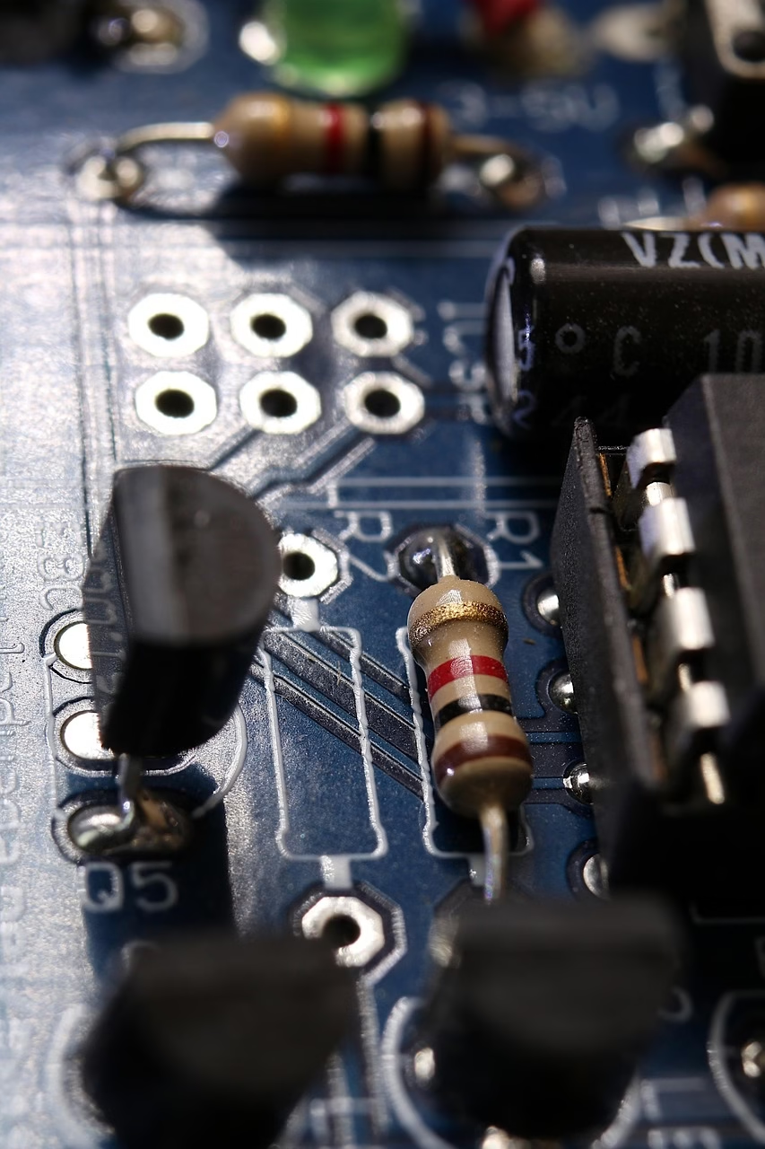
ngspice relies on “Components” to accurately model circuit behavior, necessitating the “annotation and ‘assign[ment]’ of models to individual components”. While KiCAD includes basic SPICE symbols and a PSPICE extended library, it notably “does not currently bundle any third party SPICE libraries”. Consequently, for simulating “real-world” components such as specific transistors (e.g., 2N3904, BC546, BC817) or operational amplifiers (e.g., OPA1641, TL072), designers must acquire SPICE models directly “from manufacturers’ websites”. These manufacturer-provided models are crucial as they are designed to replicate “the properties and nuances of their real-life counterparts”.
2. Crucial Steps: Model Acquisition, Pin Assignment, and Verification
The process of integrating SPICE models involves several critical steps:
- Model Acquisition: The process begins with downloading .lib (library) files from component manufacturers. It is a recommended best practice to copy these model files directly into the KiCAD project directory rather than linking to them from distant or shared folders. This practice prevents issues related to file paths or accessibility, ensuring that all necessary files are self-contained within the project.
- Pin Assignment: This step is a frequent source of errors and frustration. KiCAD schematic symbols often have pin numbering or ordering that differs from the internal pin sequence defined within a manufacturer’s SPICE model. After attaching a model to a symbol, it is imperative to open the ‘Pin Assignments’ window within the ‘Simulation Model Editor’. Here, one must meticulously “match the ‘Symbol Pin’ column (which is fixed) with the ‘Model Pin’ column (which is modifiable) so that collector meets collector, base meets base, and emitter meets emitter in the same row”. Failure to correctly map pins can lead to nonsensical simulation results or even convergence issues like “timestep too small” errors. This issue points to a fundamental “impedance mismatch” between KiCAD’s primary function as a PCB design tool, where symbols are tied to physical footprints, and its secondary role as a simulation GUI, where symbols need to map to abstract SPICE models. A symbol designed for a physical footprint might have pins ordered for ease of routing or physical layout, not necessarily for a standard SPICE model’s internal node order (e.g., C-B-E for a BJT). This structural divergence necessitates a dedicated, meticulous pin-mapping verification step in the simulation workflow, as it is a critical, yet often overlooked, determinant of simulation accuracy.
- Verification: Following model attachment and pin assignment, it is crucial to perform simple, targeted simulations to verify that the model behaves as expected and aligns with the component’s datasheet specifications.
The challenge of acquiring accurate SPICE models, particularly for newer or specialized components, has led to suggestions for leveraging artificial intelligence (AI) to generate these models. If AI can effectively generate accurate SPICE models from datasheets, component characteristics, or even real-world measurement data, it could democratize advanced simulation. This would make simulation accessible for a much broader range of components, including custom or legacy parts that lack official SPICE support, thereby significantly lowering a major barrier to entry for complex circuit analysis. Beyond accessibility, AI-generated models could potentially include more accurate representations of parasitic elements , leading to simulations that more closely mirror real-world physical behavior. This would fundamentally transform the model acquisition and validation process, shifting the designer’s focus from laborious model hunting and debugging to higher-level design verification and optimization.
D. Setting Up Your First Simulation: A Step-by-Step Walkthrough
1. Placing SPICE-Compatible Components and Sources
Unlike generic KiCAD symbols, ngspice requires specific SPICE-compatible voltage and current sources, as well as ground references. These essential simulation components are typically found within the dedicated pspice and simulation_spice libraries. For instance, a DC voltage source (VDC) or a pulsed voltage source (VPULSE) from the Simulation_SPICE library must be used instead of standard KiCAD power symbols. Conversely, common passive components like resistors (R) and capacitors (C) are generally recognized by ngspice without requiring special model assignments.
2. Defining Ground References and Power Supplies
A fundamental requirement for all SPICE simulators, including ngspice, is the presence of a defined “0V reference potential” or ground. All circuit voltages are calculated relative to this ground reference. The 0 or GND symbol, typically found in the Simulation_SPICE library, is therefore an essential inclusion in any schematic intended for simulation. A common error encountered by beginners is a “missing ground connection”. While KiCAD’s Electrical Rules Check (ERC) utilizes PWR_FLAG symbols for power nets, ngspice typically handles the GND net automatically, internally mapping it to 0.
3. Implementing Simulation Directives and Control Statements
To define the type of simulation (e.g., AC, Transient) and its specific parameters, designers can embed text-based “directives” directly onto the schematic canvas. For example, .ac dec 10 1 100k specifies an AC sweep, while .tran 1u 10m defines a transient analysis. Although the simulator window provides a user-friendly interface for setting these parameters, placing directives directly on the schematic ensures they are “retained between separate simulations” and offers the significant advantage of “seeing your statements up front when you open the schematic”. For advanced users, ngspice’s powerful control language can be accessed via .control sections for scripting complex simulation sequences and post-processing.
This persistence is paramount for ensuring project reproducibility and facilitating collaboration. When simulation parameters are solely configured within a GUI, they are prone to being lost, misunderstood, or inconsistently applied across different sessions or by different team members. Embedding these critical directives directly into the schematic transforms the simulation setup into a self-documenting artifact. This practice significantly enhances the integrity and reliability of the design process, especially in professional environments where designs undergo multiple iterations and handovers.
III. Strategic Circuit Slicing for Optimized Simulation Performance
A. The Imperative of Modular Simulation for Complex Schematics
For large and intricate designs, attempting to simulate the “whole circuit” is frequently inefficient, computationally intensive, and often unnecessary. The prevailing best practice advocates for simulating “small parts” or “small sub-circuits”. This modular approach allows designers to concentrate their debugging efforts on specific functional blocks, such as an ADC buffer stage, a power supply filter, or a digital logic section, where potential issues are suspected. This strategy dramatically reduces simulation run times and optimizes memory consumption.
This approach signifies a fundamental shift in how simulation is used—from a final, monolithic validation step to an agile, iterative, and diagnostic tool integrated throughout the design process. If a full circuit simulation fails, pinpointing the root cause can be exceedingly difficult. By simulating isolated blocks, designers can achieve faster iteration cycles, more precise fault isolation, and highly targeted design improvements. This transforms simulation into a powerful diagnostic instrument, enabling continuous refinement rather than just a pass/fail gate.
B. Identifying and Isolating Logical Circuit Blocks
Effective circuit slicing begins with the logical partitioning of the schematic into distinct “modules” or “blocks”. Examples include power supply units, microcontroller sections, input/output interfaces, or specific signal processing stages. While there are no rigid rules for this division, it should intuitively follow the functional and structural organization of the overall project. This practice is analogous to organizing source code in software development, where modularity enhances clarity and maintainability.
This connection underscores that good schematic design transcends mere drawing; it is an act of engineering a coherent system. Just as modularity in software facilitates debugging, reusability, and collaborative development, applying these principles to hardware design—especially through hierarchical schematics—creates circuits that are inherently easier to simulate, debug, and maintain. A circuit that is “sliceable” for simulation is, by definition, a well-structured and well-engineered circuit.
C. Practical Techniques for Sub-circuit Simulation
1. Leveraging the “Exclude from Simulation” Attribute (Component and Sheet Level)
KiCAD provides a powerful “Exclude from simulation” attribute, which can be applied to individual components or, in more recent versions (e.g., KiCAD V8.99), to entire hierarchical sheets. This attribute allows designers to selectively prevent specific parts of the schematic from being included in the ngspice netlist generated for simulation. While manually applying this to numerous individual components can be cumbersome , the sheet-level exclusion offers significant utility for isolating “large, non-simulatable sections like PCB parts or motor controllers”. Future KiCAD developments may include scripting capabilities to further automate the manipulation of these exclusion flags.
The evolution of the “Exclude from simulation” feature from component-level control to include sheet-level control reflects KiCAD’s ongoing adaptation to the increasing complexity of modern electronic designs, particularly those involving mixed-signal or mixed-domain (e.g., analog, digital, power, RF) elements. By providing sheet-level exclusion, the tool supports higher-level abstraction in simulation control, moving beyond individual components to entire functional modules. This directly streamlines the testbench creation process for modular simulation, reinforcing the “slicing” strategy by enabling efficient isolation of relevant circuit sections.
2. Designing Dedicated Simulation Testbenches for Isolated Modules
A highly effective practice for focused simulation is to establish “a project especially made for the simulation”. This often involves copying a “part of a schematic to another project for simulation” or, more elegantly, isolating the simulatable sub-circuit within its own hierarchical sheet. This individual sheet can then be opened “outside of the project” by directly launching its .kicad_sch file with the KiCAD Schematic Editor, enabling isolated simulation. This “separate test project is reassuring that part is working”. Testbenches for these isolated modules typically incorporate ideal sources and loads to provide controlled inputs (e.g., VSIN for AC, VPULSE for transient steps) and appropriate terminations for outputs, ensuring the sub-circuit is simulated under defined conditions.
The workflow described for simulating individual hierarchical sheets involves closing the main project and opening the .kicad_sch file directly. This is explicitly called a “workaround” and “not a great user experience”. This indicates that the built-in simulator in KiCAD currently operates on the entire project’s netlist by default, lacking a direct “simulate current sheet” option within the project context. This highlights a current limitation in KiCAD’s simulation integration, where its powerful hierarchical schematic capabilities are not fully matched by seamless, in-project sub-sheet simulation control. While the hierarchical structure inherently supports modular design, the simulation workflow currently requires users to employ a less intuitive, file-system-based approach. This points to a key area for future KiCAD development, aiming to further integrate simulation deeply into the hierarchical design flow.
3. Managing Distinct KiCAD Configurations for PCB Layout vs. Simulation
For highly specialized or complex projects, some advanced users adopt the practice of maintaining “separate configurations (with separate library sets) for PCB design and for simulations”. This allows for a clear distinction: PCB design libraries contain symbols primarily focused on footprints and physical layout, devoid of SPICE models, while simulation-specific libraries are populated with symbols that have accurate SPICE models but may lack footprint assignments. This segregation helps prevent conflicts and ensures that the appropriate model information is presented to the respective design toolchain (PCB layout vs. SPICE simulation).
This practice reveals a deeper truth about Electronic Design Automation (EDA) tools: despite efforts towards integration, the fundamental requirements for physical layout and electrical behavior analysis remain distinct. A symbol optimized for a PCB footprint (e.g., pin arrangement for routing) may not align with the internal node ordering of a SPICE model. Maintaining separate configurations is a practical, expert-level approach to manage this inherent duality, ensuring that the correct, specialized data is provided to each stage of the design process, thereby maximizing accuracy and efficiency in both domains.
IV. Proficient Hierarchical Schematic Design for Error-Free Simulation
A. Harnessing Hierarchy: Structuring Large-Scale Electronic Designs
Hierarchical schematics represent a cornerstone feature in KiCAD for effectively “partition[ing] your schematic into bigger logical blocks”. This powerful capability enables designers to break down overwhelmingly complex designs into smaller, more manageable sub-sheets, organized under a “root sheet”. This approach significantly enhances clarity, improves overall organization, and promotes design reusability, mirroring the benefits of modular programming paradigms. KiCAD supports various hierarchical structures, including flat hierarchies, simple hierarchies (each sheet used once), and complex hierarchies (sheets used multiple times).
B. Understanding Label Types and Their Impact on Netlist Generation
KiCAD provides three distinct types of labels, each with a specific connection scope, which critically impacts how nets are generated for SPICE simulation :
- Local Labels: These labels establish connections exclusively within the boundaries of the current schematic sheet. Crucially, two local labels bearing the same name on different sheets will not form a common net.
- Global Labels: Global labels create connections across the entire schematic, irrespective of sheet boundaries. All global labels sharing the same name are considered part of a single, unified net throughout the entire KiCAD project.
- Hierarchical Labels: These are specifically designed for establishing connections between a subsheet and its immediate parent sheet. They interface with “hierarchical sheet pins” placed on the corresponding block symbol on the parent sheet.
When ngspice processes a hierarchical schematic, it “flattens” the hierarchy into a single netlist. During this process, local labels from subsheets are typically prefixed with the subsheet’s name, often separated by a forward slash (e.g., /Amplifier/op_out for a local label op_out within an Amplifier subsheet). While modern ngspice versions generally handle these prefixed names, issues can arise, particularly when attempting to reference or manipulate such labels within .control sections of the simulation script.
The distinctions between local, global, and hierarchical labels are a common source of confusion for KiCAD users, especially when they begin working with multi-sheet designs. The choice of label type directly dictates how nets are connected in the generated SPICE netlist, which in turn profoundly affects simulation behavior. Misunderstanding these distinctions can lead to subtle yet critical connectivity errors that are difficult to diagnose. The following table clarifies the purpose and behavior of each label type, providing a quick guide to ensure correct netlist generation and predictable simulation outcomes, thereby helping to avoid common mistakes.
Table 2: Hierarchical Labels vs. Global Labels: Connection Scope and Best Use Cases
|
Label Type |
Connection Scope |
Best Use Cases in Hierarchical Design |
SPICE Netlist Implication |
|---|---|---|---|
|
Local Label |
Within the current schematic sheet only. |
Internal connections within a specific functional block. |
Net name prefixed with subsheet path (e.g., /SubsheetName/LocalNet). |
|
Global Label |
Across all sheets in the entire project. |
Power rails (VCC, GND), global control signals, main clock lines. |
Forms a single net across the entire flattened netlist. |
|
Hierarchical Label |
Between a subsheet and its parent sheet. |
Defining inputs/outputs of a reusable block, connecting modules in a hierarchical structure. |
Maps to corresponding hierarchical pins on the parent sheet’s block symbol. |
C. Implementing Modular Design with Hierarchical Sheets
1. Representing Sub-circuits as Reusable Hierarchical Blocks
Hierarchical sheets provide an elegant mechanism for creating reusable “virtual components” or “blocks” that can be instantiated on a parent schematic sheet. This means that a complex functional sub-circuit, such as a power supply module or a specific filter stage, can be designed once in its own dedicated sheet and then incorporated multiple times into a larger design simply by placing its hierarchical block symbol. This approach significantly promotes design reuse, reduces schematic clutter, and simplifies the overall complexity of the design.
This inherent modularity for physical design directly translates into significant advantages for simulation. A circuit that is already well-architected into distinct, functional blocks for PCB layout becomes naturally amenable to modular simulation. The clearly defined interfaces (hierarchical pins) for these blocks make it straightforward to create targeted testbenches that connect to these specific inputs and outputs, thereby streamlining the simulation setup process for complex designs and reinforcing the “slicing” strategy.
2. Establishing Robust Connections with Hierarchical Labels and Pins
Connections between a hierarchical subsheet and its parent sheet are meticulously established using hierarchical labels within the subsheet, which correspond to hierarchical sheet pins on the parent sheet’s block symbol. It is imperative to periodically “Sync hierarchical sheet pins and hierarchical labels” to ensure consistency and prevent connectivity errors, especially after modifications to the subsheet’s external interfaces.
D. Best Practices for Hierarchical Simulation Workflows
1. Simulating Individual Hierarchical Sheets within a Project
As previously noted, a common workaround for simulating a single hierarchical sheet in isolation involves a specific file-based approach: “close the project, then using the normal Windows file explorer, right-click on the individual sheet filename, and select Open With->KiCad Schematic Editor 8.0 and then run the simulation”. This effectively allows the sheet to be simulated as a standalone entity. It is important to acknowledge that there is an active feature request within the KiCAD development community for a more integrated “subsheet-only” simulation option, which would eliminate this workaround.
2. Navigating Multi-level Hierarchy in Simulation
For designs with multiple layers of hierarchy (e.g., a three-layer structure where simulatable sub-circuits reside at the lowest layer and are interconnected in a middle layer), the “exclude from simulation” attribute can be strategically employed to isolate the desired level of analysis. The topmost, non-simulatable layer of the hierarchy might be entirely excluded from the simulation netlist.
3. Addressing Common Issues with Hierarchical Net-Labels
While ngspice generally manages hierarchical net-labels (e.g., /Amplifier/op_out) during netlist flattening, certain issues can arise, particularly when attempting to access or manipulate these labels within .control sections of the simulation script. Designers have reported “unexpected simulation behavior,” such as flat or arbitrary output voltages, after adding or deleting hierarchical labels. This indicates that hierarchical labels, despite their schematic utility, can introduce subtle errors or inconsistencies in the underlying SPICE netlist. This finding suggests that the automatic flattening process (where ngspice prefixes local labels with subsheet names ) might not always be perfectly robust, or it might interact unexpectedly with specific SPICE directives or complex component models. Therefore, even with meticulous hierarchical design, expert users must remain vigilant about the integrity of the generated netlist, especially when debugging inexplicable simulation results, and be prepared to manually inspect the .cir file for discrepancies.
V. Advanced Troubleshooting and Common Pitfalls in KiCAD SPICE Simulation
A. Diagnosing and Resolving “Timestep Too Small” Errors
1. Root Causes: Rapid Transients, Numerical Instability, Model Convergence Issues
The “timestep too small” error is arguably the “most frustrating” and frequently “misnamed” error in SPICE simulation, as it fundamentally signifies “failed to converge, minimum time step reached giving up”. This error occurs when the simulator struggles to accurately resolve rapid changes in circuit behavior, forcing it to iteratively reduce its internal time step until it reaches an unmanageably small value and terminates. Common root causes include:
- Rapidly Changing Signals: The presence of extremely fast transients, such as sharp voltage or current spikes, or steep edges in digital signals.
- High-Frequency Components or Parasitics: Small capacitances, inductances, or inherent parasitic elements within models that introduce very high-frequency oscillations or resonances, which are numerically challenging for the simulator.
- Poor Convergence in Nonlinear Components: Issues with the numerical convergence algorithms when dealing with highly nonlinear devices like diodes, transistors, or complex IC models, preventing the simulator from finding a stable solution.
- Inappropriate Time Step Settings: User-defined maximum or minimum time step parameters that are either too large (missing fast events) or too small (forcing excessive computation) for the circuit’s dynamics.
- Internal Model Problems: Faulty, incomplete, or poorly constructed SPICE models that exhibit numerical instabilities.
- Incorrect Pin Mapping or Syntax Errors: Simple user errors, such as mismapping pins when attaching a model to a symbol, or other syntax errors in SPICE directives.
- Poor Circuit Design: Schematics that are inherently unstable or poorly conditioned, making them difficult for any simulator to converge.
2. Practical Solutions: Adjusting Initial Conditions, Enhancing Circuit Stability, Optimizing Time Step Parameters
- Adjust Initial Conditions: Modify the starting points of the simulation to avoid unrealistic or difficult-to-converge states. The UIC (Use Initial Conditions) flag, added to the .tran command, can sometimes force the simulator to bypass initial operating point calculation, which can be helpful if that’s where convergence fails.
- Enhance Circuit Stability:
- Introduce small series resistors (e.g., 0.05 Ohm) with voltage sources, inductors, or in power supply paths.
- Add a small Equivalent Series Resistance (ESR) to capacitors, or small conductances in parallel with capacitors.
- Consider adding very small capacitances (e.g., 1pF) from problematic nodes to ground.
- Optimize Time Step Parameters: Adjust the tstep (time step size) and tstop (final time) values in .TRAN statements. For power circuits or highly dynamic simulations, relaxing precision constraints using .options commands can be effective. For example, .options CHGTOL=1e-12 trtol=1 abstol=100n reltol=0.01 method=gear RSERIES=0.05. CHGTOL can be varied between 1e-12 and 1e-10 (default 1e-14). Reducing RELTOL (relative tolerance) or ABSTOL (absolute tolerance) can increase accuracy but might exacerbate convergence problems.
- Model and Circuit Review: Meticulously check for correct model files and ensure the SPICE model’s pinout is correctly mapped to the KiCAD symbol. Review the circuit design for any configurations that might inherently cause extreme instability or oscillations. In some cases, substituting a problematic OpAmp with a different type that has better stability characteristics can resolve issues.
The “timestep too small” error is identified as the “most frustrating” and frequently encountered issue in SPICE simulation. This error is a symptom of various underlying problems, often interconnected. The following table serves as a comprehensive diagnostic tool, allowing users to quickly correlate their specific error symptoms with potential causes and corresponding, concrete solutions. This structured approach significantly streamlines the debugging process, reduces frustration, and directly addresses the need for troubleshooting convergence issues by providing a clear roadmap to resolution.
Table 3: Troubleshooting “Timestep Too Small” Errors: Causes and Solutions
|
Cause |
Explanation |
Solution(s) |
Relevant SPICE Options/Directives |
|---|---|---|---|
|
Rapidly Changing Signals |
Sharp voltage/current spikes, steep digital edges force tiny time steps. |
Smooth inputs, add small series resistors/parallel capacitors. |
.tran tstep tstop UIC |
|
High-Frequency Components/Parasitics |
Small L/C or parasitic elements introduce hard-to-resolve oscillations. |
Add small series resistors to inductors, ESR to capacitors, small C to GND. |
.options RSERIES=0.05 CSHUNT=1p |
|
Poor Convergence in Nonlinear Components |
Simulator struggles to find stable solution for diodes, transistors, ICs. |
Adjust initial conditions, add UIC flag, simplify models. |
.tran… UIC, .options method=gear |
|
Inappropriate Time Step Settings |
User-defined tstep/tstop values don’t match circuit dynamics. |
Adjust tstep and tstop values; relax precision for power circuits. |
.tran tstep tstop, .options CHGTOL=1e-12 RELTOL=0.01 ABSTOL=100n |
|
Internal Model Problems |
Faulty or unstable SPICE models. |
Obtain verified models, try alternative component models. |
None (model-specific issue) |
|
Incorrect Pin Mapping/Syntax Errors |
Misaligned symbol pins to model pins, or errors in directives. |
Meticulously verify pin assignments in Simulation Model Editor. Inspect netlist. |
None (schematic/syntax issue) |
|
Poor Circuit Design |
Inherently unstable or poorly conditioned circuit. |
Revise circuit design for stability, simplify complex sections. |
None (design issue) |
B. Addressing Missing Ground and Floating Node Issues
A fundamental requirement for all SPICE simulators is the presence of a defined ground (0V reference) from which all other node voltages are calculated. A “missing ground connection” is a surprisingly common oversight that can halt a simulation. Similarly, floating nodes—wires or components that are electrically unconnected to any other part of the circuit—can introduce numerical instability and lead to simulation errors.
To address these issues, always include a GND or 0 symbol, typically sourced from the Simulation_SPICE library, in your schematic. Regularly run KiCAD’s Electrical Rules Check (ERC). ERC is highly effective at identifying unconnected pins, wires not connected to anything, or multiple labels on a single node, all of which can indicate floating nodes or unintended disconnections.
C. Resolving Model-Related Discrepancies: Pin Mapping and Definition Errors
As extensively discussed, incorrect pin mapping between a KiCAD symbol and its associated SPICE model is a pervasive and critical source of simulation errors. Manifestations include errors such as “Unable to find definition of model” or inexplicable circuit behavior during simulation.
The primary solution is meticulous verification of pin assignments within the ‘Simulation Model Editor’ for every component using an external SPICE model. Ensure that the correct model file is selected and, crucially, that it is copied directly into the project directory rather than linked from a remote location. This practice prevents model loading failures due to path issues. This practical approach addresses a common operational pitfall related to file system management, especially in collaborative or long-term projects. External links can break due to changes in file paths, network drive availability, or permissions. By centralizing all SPICE model files within the project directory, the simulation setup becomes self-contained, highly portable, and significantly more robust against environmental dependencies. This enhances reproducibility and reduces debugging time associated with missing or inaccessible models. For complex models or custom subcircuits, manually inspecting the generated ngspice netlist (.cir file) can often reveal subtle errors in how KiCAD translates the schematic into a simulation-ready format.
D. A Systematic Debugging Workflow: ERC, Incremental Simulation, and Project Backups
A systematic and disciplined approach is paramount for efficient simulation debugging:
- Electrical Rules Check (ERC): Always initiate debugging by running KiCAD’s ERC. This tool is invaluable for catching fundamental connectivity errors, identifying missing power flags, and detecting unconnected pins, which are common culprits for simulation failures.
- Incremental Simulation: Adopt an incremental approach by “divid[ing] the circuit into blocks and shut[ting] them off one by one with the Attributes->Exclude from simulation”. This methodical isolation helps pinpoint the exact problematic section within a larger design. The general best practice of simulating smaller parts first is an integral part of this strategy.
- Project Backups: Implement a rigorous backup strategy. While KiCAD generates backups, it is highly recommended to “Make a backup of the the backup with a telling name when you reached progress because you will mess it up again when you are trying to find your next bug!”. This candid advice acknowledges that simulation debugging is an inherently iterative, often frustrating, and error-prone process, even for experienced users. This emphasis on meticulous backups and incremental testing underscores that simulation is a highly empirical activity where managing complexity and uncertainty is as crucial as theoretical knowledge of SPICE commands. It shifts the perception from a purely analytical task to one deeply rooted in practical, iterative problem-solving.
- Restarting: Occasionally, transient issues can be resolved by simply “restarting everything or just close the simulation window and start a new one”. This can clear lingering states or minor software glitches.
- Label Management: Organize net labels logically (e.g., supply_VCC, pwm_in, pwm_out, sensor_data). This practice makes it significantly easier to identify and select specific signals for plotting in the waveform viewer.
E. Utilizing Advanced SPICE Directives for Complex Scenarios
Beyond the basic simulation commands, ngspice offers a rich set of directives for performing advanced analyses and customizing simulation behavior. These include:
- .options: This directive allows fine-tuning of ngspice’s internal algorithms and tolerances, crucial for addressing convergence issues. Parameters like CHGTOL (charge tolerance), RELTOL (relative voltage/current tolerance), ABSTOL (absolute voltage/current tolerance), method=gear (numerical integration method), and RSERIES (series resistance added to all nodes) can be adjusted to improve stability and accuracy.
- .control sections: These powerful sections enable scripting of complex simulation sequences, allowing for automated parameter sweeps, post-processing of simulation data, and even Monte Carlo analyses. This provides a flexible environment for dynamically modifying circuit parameters and executing iterative simulations. The ability to use .control sections for scripting and Monte Carlo simulation indicates that expert-level simulation extends far beyond merely verifying basic circuit functionality. Proficiency in ngspice’s control language and the use of advanced directives like .options and .IC are gateways to sophisticated design validation. This enables comprehensive robustness analysis (e.g., how component tolerances affect performance via Monte Carlo), design optimization, and characterization under various conditions—capabilities that manual, single-point simulations simply cannot achieve. This capability transforms simulation from a simple check into a powerful predictive and optimization tool.
- Initial Conditions (.IC): Used to set specific starting voltages or currents for nodes in a transient simulation, which can be critical for guiding the simulator to a desired operating point or avoiding startup transients.
- User-defined signals: This feature allows designers to define custom signals for plotting, combining multiple node voltages or currents, or applying mathematical functions to improve waveform visualization and analysis.
VI. Conclusion: Refining Your KiCAD Simulation Expertise
A. Summary of Key Best Practices for Robust Simulation
Achieving mastery in KiCAD SPICE simulation for complex schematics hinges on several key best practices. It is essential to internalize KiCAD’s role as a sophisticated GUI for the powerful ngspice engine, understanding both its conveniences and underlying complexities. Paramount to accurate results is the meticulous sourcing of precise SPICE models and ensuring their correct pin assignment to KiCAD symbols. For managing large designs, the strategic implementation of circuit slicing and hierarchical schematic design is indispensable, allowing for modular analysis and efficient debugging. Finally, adopting a systematic approach to troubleshooting common errors—leveraging ERC, incremental simulation, and diligent project backups—is critical for navigating the iterative nature of simulation debugging. Ultimately, effective simulation is an ongoing, diagnostic process that continuously refines and validates electronic designs.
B. Future Directions and Continuous Learning Resources
The KiCAD/ngspice integration is a dynamic and continuously evolving platform, with ongoing efforts focused on improving the GUI, enhancing simulation control, and streamlining hierarchical sheet-level simulation. Designers are encouraged to remain updated with new KiCAD releases to leverage these advancements. The continuous development, including features like improved GUI interfaces and support for advanced simulation capabilities , means that “mastery” is not a static state but requires continuous adaptation. This necessitates a proactive engagement with the evolving toolset to maintain and enhance simulation proficiency.
Continuous learning is vital; users should actively explore official ngspice documentation, particularly the comprehensive User’s Manual , engage with the vibrant KiCAD and ngspice community forums , and utilize the wealth of video tutorials (such as those on Holger’s YouTube channel). Furthermore, a rich repository of simulation examples is available for various KiCAD versions, serving as invaluable learning and reference tools. By embracing these resources and the iterative nature of design and simulation, engineers can continually refine their expertise and push the boundaries of electronic circuit development.
Works cited
1. ngspice circuit simulator – stand-alone and embedded into KiCad, https://archive.fosdem.org/2024/events/attachments/fosdem-2024-2834-ngspice-circuit-simulator-stand-alone-and-embedded-into-kicad/slides/22676/ngspice-HolgerVogt_tEfhemB.pdf 2. Simulating a KiCad Circuit : 7 Steps – Instructables, https://www.instructables.com/Simulating-a-KiCad-Circuit/ 3. SPICE Simulation – KiCad, https://www.kicad.org/discover/spice/ 4. Simulation Workflow Best-Practise for a Complete Project – KiCad.info Forums, https://forum.kicad.info/t/simulation-workflow-best-practise-for-a-complete-project/53856 5. How to make clear and well organized schematics – PCB Design …, https://www.pcbway.com/blog/PCB_Design_Tutorial/How_to_make_clear_and_well_organized_schematics.html 6. Using ngspice in KiCad: Documentation, https://forum.kicad.info/t/using-ngspice-in-kicad-documentation/59318 7. Ngspice circuit simulator – Tutorials – SourceForge, https://ngspice.sourceforge.io/tutorials.html 8. KiCad 7.x SPICE Simulation – SaludPCB, https://saludpcb.com/kicad-7-x-spice-simulation/ 9. Heads up for beginners for SPICE simulation – Simulation (Ngspice) – KiCad.info Forums, https://forum.kicad.info/t/heads-up-for-beginners-for-spice-simulation/47538 10. Ngspice is always right (KiCAD-ngspice transient analysis simulation debugging), https://forum.kicad.info/t/ngspice-is-always-right-kicad-ngspice-transient-analysis-simulation-debugging/57509 11. Spice · Issue #418 · KiCad/kicad-symbols – GitHub, https://github.com/KiCad/kicad-symbols/issues/418 12. Windows Downloads – KiCad, https://www.kicad.org/download/windows/ 13. Basic simulation problem – Simulation (Ngspice) – KiCad.info Forums, https://forum.kicad.info/t/basic-simulation-problem/33287 14. Error: circuit not parsed – Simulation (Ngspice) – KiCad.info Forums, https://forum.kicad.info/t/error-circuit-not-parsed/29372 15. Performing A Circuit Simulation In KiCad – Woolsey Workshop, https://www.woolseyworkshop.com/2019/07/01/performing-a-circuit-simulation-in-kicad/ 16. Simulation directives – Simulation (Ngspice) – KiCad.info Forums, https://forum.kicad.info/t/simulation-directives/51918 17. Is this a good (or “the right”) way to design more complex circuits? – Electrical Engineering Stack Exchange, https://electronics.stackexchange.com/questions/749630/is-this-a-good-or-the-right-way-to-design-more-complex-circuits 18. Schematic Creation and Editing – KiCad Docs, https://docs.kicad.org/8.0/en/eeschema/eeschema_schematic_creation_and_editing.html 19. SPICE simulation for individual hierarchical sheets – KiCad.info Forums, https://forum.kicad.info/t/spice-simulation-for-individual-hierarchical-sheets/43068 20. Schematic Editor | 7.0 | English | Documentation – KiCad Docs, https://docs.kicad.org/7.0/en/eeschema/eeschema.html 21. Local label delimiters in spice netlists – Simulation (Ngspice) – KiCad.info Forums, https://forum.kicad.info/t/local-label-delimiters-in-spice-netlists/25877 22. Solving timestep error in KiCAD – Simulation (Ngspice) – KiCad.info …, https://forum.kicad.info/t/solving-timestep-error-in-kicad/54167 23. Schematic Editor – KiCad Docs, https://docs.kicad.org/7.0/pl/eeschema/eeschema.pdf