Abstract: Intel’s Loihi neuromorphic processor represents a significant departure from conventional Von Neumann architectures, exemplified by ARM and x64 CPUs. Inspired by the brain’s energy-efficient, event-driven computation, Loihi integrates processing and memory, enabling sparse, asynchronous, and on-chip learning capabilities. This article elucidates the fundamental architectural differences between Loihi and traditional processors, highlighting how Loihi’s unique design principles lead to qualitative advantages such as superior energy efficiency and real-time adaptability. Quantitative benchmarks, particularly in emerging AI workloads like Large Language Models, demonstrate Loihi’s potential for higher throughput and significantly lower energy consumption compared to state-of-the-art GPUs in specific inference scenarios. This analysis explores Intel’s strategic imperative for developing Loihi to address the escalating energy demands of artificial intelligence and traces its lineage from pioneering neuromorphic efforts like IBM TrueNorth and SpiNNaker, positioning Loihi as a critical step towards a more sustainable and intelligent computing future.
1. Introduction to Neuromorphic Computing and Intel Loihi
The Evolution of Computing Paradigms and the Emergence of Neuromorphic Computing
The landscape of computing has been predominantly shaped by the Von Neumann architecture since its inception in the mid-20th century. This foundational model, characterized by its stored-program concept, dictates a fundamental separation between the central processing unit (CPU) and a unified memory unit that stores both instructions and data. While this design has proven remarkably versatile, underpinning virtually all general-purpose computers, it inherently faces a significant limitation known as the “Von Neumann bottleneck.” This bottleneck arises from the continuous need to shuttle data and instructions between the CPU and memory over a shared bus, creating a performance and energy consumption constraint.
In recent decades, the rapid advancement of Artificial Intelligence (AI), particularly the development and scaling of large neural networks, has placed unprecedented demands on conventional computing architectures. These sophisticated AI workloads are inherently computationally intensive and have exacerbated the limitations of the Von Neumann model, leading to substantial energy consumption challenges. The increasing demand for energy-efficient AI systems, coupled with the observation that Spiking Neural Networks (SNNs) are “exceedingly poorly served by conventional architectures,” points to a fundamental architectural mismatch. This suggests that the current trajectory of AI scaling on existing hardware is unsustainable. Consequently, neuromorphic computing has emerged as a critical research field, drawing inspiration from the biological brain’s remarkable energy efficiency and parallel processing capabilities. The objective is to develop novel hardware architectures and algorithms that circumvent the Von Neumann bottleneck by emulating the brain’s event-driven, asynchronous, and in-memory computational principles. This represents not merely an alternative but a necessary evolution or augmentation of computing paradigms, indicating a long-term industry trend towards specialized, efficient hardware solutions to sustain the growth of computationally intensive AI, addressing both performance and sustainability concerns.
Overview of Intel Loihi (Loihi 1 and Loihi 2) as Intel’s Venture into Brain-Inspired Hardware
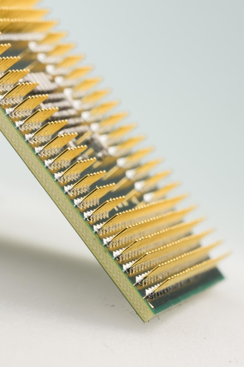
Intel’s Loihi, pronounced “low-EE-hee,” stands as a pioneering neuromorphic research chip specifically engineered to model spiking neural networks (SNNs) in silicon. The initial iteration of Loihi, first introduced in November 2017, was fabricated using Intel’s 14nm process technology. It featured 128 cores, collectively supporting approximately 130,000 artificial neurons and 130 million synapses, marking Intel’s significant entry into brain-inspired computing.
Building upon the foundations of its predecessor, Loihi 2 was released in 2021, representing a substantial leap forward in neuromorphic capabilities. Fabricated on the more advanced Intel 4 process, Loihi 2 delivers up to a tenfold increase in spike processing speed compared to the original Loihi chip. A single Loihi 2 chip significantly expands capacity, supporting up to 1 million neurons and 120 million synapses. Key enhancements in this second generation include the ability to implement custom neuron models using microcode instructions, the introduction of “graded spikes” that can encode up to 32-bits of data (a significant upgrade from the 1-bit spikes of Loihi 1), and improved asynchronous networking capabilities designed for seamless multi-chip scaling.
Intel’s commitment to advancing neuromorphic computing extends beyond hardware development. Intel Labs actively fosters a collaborative environment through the Intel Neuromorphic Research Community (INRC), providing global research groups with access to Loihi-based systems via a cloud-based platform. This initiative aims to accelerate innovation in the field, with Intel offering various forms of support, including hardware, academic grants, and invitations to community workshops. The rapid and substantial generational improvements from Loihi 1 to Loihi 2, coupled with the development of the open-source Lava framework for neuro-inspired applications and the nurturing of the INRC, underscore Intel’s deep and sustained commitment to this emerging field. This indicates that neuromorphic computing is not a fleeting experimental project for Intel but a strategic, long-term investment aimed at establishing leadership in a new computing paradigm.
The Driving Forces Behind Neuromorphic Research, Particularly in the Context of AI’s Energy Demands
The primary impetus behind the development of neuromorphic computing is the escalating demand for more energy-efficient artificial intelligence systems. Conventional AI models, especially large language models (LLMs), are characterized by their immense computational requirements, translating into substantial energy consumption for both their training and inference phases. The computational and energy demands of LLMs, for instance, are enormous, motivating the development of efficient and scalable foundation models that are not only algorithmically optimized but also co-designed with novel hardware architectures.
Loihi directly addresses this critical challenge by leveraging several brain-inspired principles. Its design incorporates temporal sparsity, meaning computation is performed only when there are significant changes to the input, and spatial sparsity, where only a limited subset of neurons activate. Furthermore, Loihi integrates compute capabilities directly within or very near memory units. This architectural approach minimizes unnecessary computations and drastically reduces data movement, which is a major source of energy consumption in traditional systems, thereby leading to significant energy savings. The pervasive emphasis on “energy-hungry AI” and Loihi’s architectural features—such as sparsity, event-driven processing, and compute-near-memory—reveal that energy efficiency and sustainability are not merely secondary benefits but are fundamental design principles driving neuromorphic research. This signifies a strategic shift in hardware design priorities from solely maximizing peak performance, often measured in floating-point operations per second (FLOPS), to optimizing for performance-per-watt and long-term operational costs. This positions neuromorphic computing as a crucial component of “green AI” and a vital solution for the future of computationally intensive AI.
2. Foundational Architectures: Von Neumann (ARM & x64) vs. Neuromorphic (Loihi)
2.1. The Von Neumann Model: Principles of ARM and x64 Processors
The Von Neumann architecture, also referred to as the stored-program concept, forms the bedrock of virtually all modern general-purpose computers, including those powered by ARM and x64 processors. A defining characteristic of this architecture is the unified memory space where both program instructions and data are stored. This shared memory enables a high degree of flexibility, allowing for self-modifying code and facilitating the development of sophisticated programming tools like compilers and assemblers.
Processors adhering to the Von Neumann model execute instructions sequentially through a repetitive cycle known as the Fetch-Decode-Execute (FDE) cycle. During this cycle, a central control unit retrieves instructions and data from the shared memory. These instructions are then decoded, and the specified operations are performed by an Arithmetic Logic Unit (ALU), utilizing various internal registers for temporary storage. The rate at which a processor can complete these FDE cycles is dictated by its clock speed; for instance, a 3.5GHz processor can process 3.5 billion instructions per second.
A fundamental aspect of the Von Neumann architecture is the physical separation between the Central Processing Unit (CPU) and the main memory. This separation necessitates continuous data transfer between these two components via a shared bus, leading to the well-known “Von Neumann bottleneck”. This bottleneck inherently limits system performance, as instruction fetches and data operations cannot occur simultaneously over the single shared bus. While modern processors employ various mitigation techniques, such as multi-level cache hierarchies (often with separate caches for instructions and data closest to the CPU), the underlying architectural constraint persists.
ARM processors represent a family of Reduced Instruction Set Computing (RISC) architectures. They are widely recognized for their exceptional energy efficiency, scalability, and pervasive adoption across a diverse range of devices, from smartphones and wearables to embedded systems and even supercomputers. Their efficiency stems from a simplified instruction set, which allows for faster execution and lower power consumption per computational operation, further enhanced by techniques like pipelining. ARM Holdings licenses its architectural designs, fostering a vast global ecosystem that develops specialized chips optimized for specific applications. Contemporary ARM processors also incorporate multi-core designs, enabling high performance for parallel processing applications.
In contrast, x64 processors, predominantly associated with Complex Instruction Set Computing (CISC) architectures, are the cornerstone of general-purpose computing, high-performance desktops, and data centers. These processors, manufactured by companies like Intel and AMD, prioritize raw computational power and versatility. They are characterized by very high clock speeds, multiple processing cores, and extensive multi-level cache memory, all designed to maximize throughput for a wide array of computational tasks.
Despite their versatility and power, conventional Von Neumann architectures face inherent limitations when confronted with the unique demands of Spiking Neural Network (SNN) models. SNNs are described as being “exceedingly poorly served by conventional architectures”. The synchronous, clock-driven operation and the persistent Von Neumann bottleneck lead to significant inefficiencies when processing the sparse, event-driven, and massively parallel computations that are characteristic of SNNs. Traditional processors, with their wide data paths, deep pipelines, and high memory access latencies, are optimized for dense, predictable data streams and batched computations. This operational modality often does not align with the dynamic and sparse nature of neuromorphic workloads, resulting in wasted energy and computational cycles. The fundamental differences in how Von Neumann (ARM/x64) and neuromorphic (Loihi) architectures handle data, communication, and computation reveal a profound architectural mismatch for certain AI tasks. It is not merely a matter of speed but of computational philosophy. Von Neumann processors are designed for dense, continuous data processing, whereas neuromorphic systems excel at sparse, event-triggered operations. This inherent divergence means that even with advanced optimizations, conventional processors will struggle to achieve the same levels of energy efficiency and real-time responsiveness for true SNN workloads.
2.2. Intel Loihi’s Neuromorphic Architecture: A Biological Inspiration
Intel’s Loihi processor is a testament to the profound influence of biological neuroscience on novel hardware architectures and algorithms. Its design is meticulously crafted to emulate the brain’s remarkable energy efficiency and complex behaviors, departing significantly from the traditional Von Neumann paradigm.
At its core, Loihi operates on several key principles inspired by the brain:
- Event-Driven Computation: Unlike the synchronous, clock-driven operations of conventional processors, Loihi’s computations are triggered by discrete “spikes” or impulses generated by individual neurons. This event-driven nature means that processing resources are only activated when there is meaningful input activity, leading to substantial energy savings, particularly when processing sparse data.
- Spiking Neural Networks (SNNs): Loihi is purpose-built for Spiking Neural Networks, a neural network model where information is encoded not just in the strength of connections but crucially in the timing of these single-bit impulses. This temporal encoding allows for efficient representation of dynamic information.
- In-Memory Processing (Compute-Near-Memory): Loihi adopts a distributed, “in-memory computing” approach, fundamentally addressing the Von Neumann bottleneck. Each neuromorphic core on Loihi integrates its own local Static Random-Access Memory (SRAM) for storing neuron states and synaptic weights. This co-location of computation and memory drastically reduces the need for energy-intensive data movement between separate processing and memory units, thereby improving both latency and overall energy efficiency. This represents a radical, fundamental solution to a long-standing problem in computing, as it drastically reduces the energy and time spent on data movement.
- Asynchronous Communication: Communication within Loihi’s architecture is entirely asynchronous and event-driven. Neurons communicate by sending discrete “spike messages” only when they fire, utilizing an on-chip network. This Address Event Representation (AER) scheme ensures that only active neurons generate communication traffic, leading to significantly lower data movement and power consumption compared to the continuous, synchronous bus-based communication of traditional systems. This selective activation is a primary driver of its exceptional energy efficiency and real-time responsiveness for specific, event-based workloads.
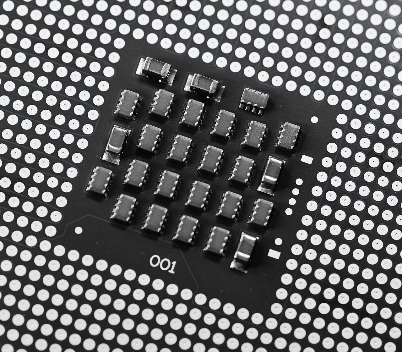
Loihi’s architecture is composed of several specialized components. Loihi 2, for instance, features 128 fully asynchronous neural cores. These cores function as programmable digital signal processors, meticulously optimized for emulating biological neural dynamics, and are equipped with specialized memory structures tailored for network connectivity. Beyond fixed neuron models, these cores now support user-defined arithmetic and logic, enabling the implementation of custom neuron behaviors via microcode. A notable advancement in Loihi 2 is the introduction of “graded spikes,” which can encode integer data payloads up to 32-bits, in addition to the traditional 1-bit spikes. This enhancement allows for richer information representation and facilitates the conversion of conventional Artificial Neural Networks (ANNs) to SNNs with minimal accuracy loss.
A crucial and pragmatic element of Loihi’s design is the inclusion of conventional Von Neumann processors. Loihi 2 incorporates six Lakemont x86 cores at the periphery of its neuromorphic mesh. These x86 cores are vital for handling essential management tasks, data input/output, and network configuration. Critically, they act as a bridge, converting data between the dense, synchronous encodings typical of conventional computing and the sparse, event-based representations inherent to the neuromorphic domain. This deliberate inclusion of conventional cores alongside specialized neuromorphic cores is a strategic design choice, highlighting Intel’s pragmatic approach. It signifies that Loihi is not intended as a complete replacement for general-purpose computing but rather as a powerful, specialized accelerator that can seamlessly interface with and augment existing Von Neumann systems. This hybrid architecture facilitates practical deployment by offloading non-neuromorphic tasks to the x86 cores, thereby accelerating the adoption of this new computing paradigm and making it more accessible for real-world applications.
Communication between neural cores and support for multi-chip scaling are facilitated by an asynchronous network-on-chip (NoC). This NoC enables the construction of large-scale neuromorphic systems, such as Pohoiki Springs, which integrates 768 Loihi chips to collectively implement 100 million spiking neurons.
One of Loihi’s most distinctive features is its ability to perform “on-chip learning” through integrated “programmable synaptic learning rules”. This capability allows the chip to dynamically reconfigure synaptic connections and adapt to new stimuli directly on the silicon. Consequently, SNNs implemented on Loihi can become “smarter” over time without the need for conventional, off-chip training, which typically involves computationally intensive backpropagation algorithms. These learning rules are designed to operate using only locally available information, such as spike trains from neighboring neurons, ensuring that synaptic weights are modified efficiently and in a well-defined manner. Loihi supports features like configurable spike traces and additional synaptic state variables to enhance the flexibility of these learning mechanisms.
3. Step-by-Step Architectural Differences: Loihi vs. ARM/x64
The architectural divergence between Intel’s Loihi and conventional ARM or x64 processors is profound, reflecting fundamentally different approaches to computation. Understanding these distinctions is crucial for appreciating Loihi’s unique advantages and its potential to redefine specific computing paradigms.
Data Representation and Processing
In conventional Von Neumann architectures, exemplified by ARM and x64 processors, data is primarily represented and processed using high-precision numerical values. This typically involves fixed-point or floating-point numbers, often encoded with 32-bit or 64-bit precision. Computation on these processors involves complex arithmetic operations, such as matrix multiplications and divisions, performed in a dense and continuous fashion. Every bit of data is actively processed, even if it represents a zero or an inactive state.
In stark contrast, Loihi fundamentally processes information through discrete, event-based “spikes”. In the original Loihi, these were single-bit impulses, where the primary information was encoded in the timing of the spikes and the identity of the neuron that fired. Loihi 2 significantly advances this by introducing “graded spikes,” which can encode integer data payloads up to 32-bits. This enhancement allows for a richer representation of information per event, facilitating the conversion of conventional Artificial Neural Networks (ANNs) to SNNs with minimal accuracy loss. The core principle, however, remains low-precision, event-driven computation. This shift from high-precision numerical values to sparse, timed spikes (and later graded spikes) represents a paradigm change in information encoding. This enables Loihi to achieve significant energy efficiency by performing computation only when a meaningful “event” (spike) occurs. The evolution to graded spikes in Loihi 2 indicates a pragmatic step towards broader applicability and easier integration with existing AI models, bridging the gap between traditional numerical computation and the sparse, event-driven world of neuromorphic systems.
Communication Paradigm
Communication within and between components in ARM and x64 Von Neumann processors is predominantly synchronous, meticulously orchestrated by a global clock signal. Data is transferred in blocks over shared buses, necessitating that all components operate in precise lockstep. While this synchronous approach ensures predictable timing and simplifies design complexity for general-purpose tasks, it can lead to considerable energy waste. Components, even when idle or not performing useful work, must still be clocked, consuming power for clock distribution and maintaining internal states.
Loihi, conversely, employs an asynchronous, event-driven communication model. Neurons communicate by sending discrete “spike messages” only when they fire. This “Address Event Representation (AER)” mechanism means that communication traffic is generated solely by active neurons. This drastically reduces the amount of data movement and power consumption compared to the continuous data transfer inherent in synchronous systems. The asynchronous, event-driven communication of Loihi is a critical source of its energy efficiency. Unlike clock-driven systems that consume power even when components are idle, Loihi’s components only activate and consume significant power when a spike event occurs. This “compute only when necessary” principle is highly effective for processing sparse, real-world data, where only a fraction of the network might be active at any given moment, leading to substantial energy savings.
Memory and Computation Integration
A defining characteristic of the Von Neumann architecture is the fundamental separation of the central processing unit (CPU) and a distinct, centralized memory unit. Data and instructions must be fetched from this shared memory, processed by the CPU, and results are often written back to memory. This constant shuttling of data across the “Von Neumann bottleneck” is a primary limitation for both performance and energy efficiency, as memory access often becomes the limiting factor in overall system speed.
Loihi adopts an “in-memory computing” or “compute-near-memory” architecture, which fundamentally re-imagines this separation. Each neuromorphic core on Loihi integrates its own local memory, typically Static Random-Access Memory (SRAM), dedicated to storing neuron states and synaptic weights. This distributed, hypergranular memory access ensures that computation happens directly where the data resides, minimizing energy-intensive data movement and significantly reducing memory access latency. This effectively addresses the Von Neumann bottleneck by eliminating the need for extensive data transfer between physically separate processing and memory units. Loihi’s distributed, compute-near-memory architecture is a radical, fundamental solution to the Von Neumann bottleneck. Instead of attempting to mitigate the bottleneck with faster buses or larger caches, Loihi re-architects the entire compute model by co-locating processing elements and their associated memory. This has profound implications for latency and energy consumption, particularly for sparse, graph-like computations typical of neural networks, as it drastically reduces the energy and time spent on data movement.
Operational Modality
Conventional ARM and x64 processors operate on a dense, continuous instruction execution model. Even when processing sparse data, these processors often fetch and operate on entire blocks of data, performing computations on many elements, including zeros, in a predictable, batched manner to maintain pipeline efficiency. This approach, while efficient for dense, structured data, can lead to significant wasted computation and energy when dealing with naturally sparse workloads.
In contrast, Loihi is optimized for sparse and non-batched computation. Its event-driven nature means that computation is triggered only by active spikes, leading to “temporal sparsity,” where computation occurs only when input changes, and “spatial sparsity,” where only a subset of neurons activate. This makes Loihi inherently efficient for processing real-world, dynamic data streams that are often naturally sparse, such as sensory inputs or event-based data. Loihi’s operational modality, driven by its inherent sparsity, signifies that it expends energy and computational cycles only when there is meaningful activity. This contrasts sharply with the “always on” or “batch processing” nature of conventional processors that may process large amounts of irrelevant or zero data. This selective activation is a primary driver of its exceptional energy efficiency and real-time responsiveness for specific, event-based workloads.
Learning and Adaptability
In traditional computing paradigms utilizing ARM or x64 processors, machine learning models are typically trained off-chip on large datasets using computationally intensive algorithms like backpropagation. This training phase often leverages specialized hardware such as GPUs or dedicated AI accelerators. Once trained, the model’s fixed weights are then deployed for inference. While some forms of online learning can be implemented in software on these processors, continuous, on-chip adaptation is not an inherent architectural feature of the CPU itself.
Loihi, however, stands apart with its integrated “programmable synaptic learning rules” that enable intrinsic on-chip learning and adaptation. Spiking Neural Networks on Loihi can dynamically remap synapses in response to stimuli and become “smarter” over time without the need for conventional, batch-based training cycles. This local, activity-dependent plasticity allows for continuous learning directly on the hardware, making it exceptionally well-suited for adaptive AI at the edge. These learning rules are designed to operate using only locally available information, such as spike trains from neighboring neurons, ensuring that synaptic weights are modified efficiently and in a well-defined manner. The on-chip learning capability is one of Loihi’s most transformative advantages. It shifts the paradigm from static, pre-trained inference models to truly adaptive, autonomous AI systems that can learn and evolve in real-time within resource-constrained edge environments. This capability is crucial for applications where continuous adaptation to novel stimuli is essential, reducing reliance on cloud-based retraining, minimizing data transfer, and enhancing privacy and responsiveness.
Table 1: Comparative Architectural Principles: Loihi vs. Von Neumann (ARM/x64)
| Feature | Von Neumann (ARM/x64) | Neuromorphic (Loihi) |
|---|---|---|
| Architecture Paradigm | Stored-program, Clock-driven | Brain-inspired, Event-driven |
| Data Representation | Numerical (e.g., 32/64-bit fixed/floating-point) | Spikes (1-bit, Loihi 2: up to 32-bit graded spikes) |
| Communication | Synchronous, Bus-based, Global Clock | Asynchronous, Event-driven Spike Messages (AER) |
| Memory-Compute Model | CPU-Memory Separate (Von Neumann Bottleneck) | Compute-Near-Memory (Distributed, Local SRAM) |
| Operational Modality | Dense, Batched, Continuous Instruction Execution | Sparse, Non-batched, Event-triggered Activation |
| Learning/Adaptability | Off-chip, Backpropagation-based Training | On-chip, Local Synaptic Plasticity (Programmable Rules) |
4. Performance Outperformance: Qualitative and Quantitative Analysis
Intel’s Loihi neuromorphic processor demonstrates significant performance advantages over conventional ARM or x64 processors in specific domains, both qualitatively through its unique architectural principles and quantitatively through empirical benchmarks.
4.1. Qualitative Advantages of Loihi’s Architecture
Loihi’s brain-inspired architecture confers several distinct qualitative advantages, redefining what “performance” means for certain AI workloads.
- Superior Energy Efficiency: Loihi’s event-driven, sparse computation, coupled with its compute-near-memory architecture, inherently leads to significantly lower power consumption compared to conventional processors, especially for Spiking Neural Network (SNN) workloads. It leverages temporal and spatial sparsity, consuming power only when neurons spike, which is particularly advantageous for real-world, dynamic data streams where activity is often sparse. Intel has indicated that Loihi can be “1000 times more energy efficient than general-purpose computing systems used to train neural networks” in specific contexts. This emphasis on energy efficiency and sustainability is a fundamental design principle, critical for the future of ubiquitous, embedded AI.
- Real-time Processing and Low Latency: The asynchronous, event-driven nature of Loihi enables it to process information with very low latency. Computations are triggered immediately by incoming spikes, eliminating the need to wait for global clock cycles or batch completions common in Von Neumann systems. This capability is crucial for real-time intelligent signal processing and applications demanding deterministic responses, such as those in embedded control systems or robotics.
- Adaptive and On-chip Learning: As previously discussed, Loihi’s programmable synaptic rules facilitate continuous, unsupervised learning directly on the chip. This allows the system to adapt to new data and environments in real-time, enabling it to become “smarter” over time without requiring external retraining cycles. This is a significant advantage for autonomous edge AI, where continuous adaptation to novel stimuli is essential, reducing reliance on cloud-based retraining, minimizing data transfer, and enhancing privacy and responsiveness.
- Robustness to Noise and Uncertainty: By encoding information in spike timing and leveraging distributed processing, SNNs on Loihi can exhibit greater resilience to noise and uncertainty, mirroring the robustness observed in biological systems. For instance, Loihi has demonstrated the ability to learn and recognize hazardous chemicals even in the presence of significant noise and occlusion. This capability is vital for real-world applications where data quality can be inconsistent.
- Scalability for Large Networks: Loihi’s modular architecture, with its network-on-chip and asynchronous communication, is designed for multi-chip scaling. Systems like Pohoiki Springs, which integrate 768 Loihi chips, can collectively implement 100 million spiking neurons. Loihi 2 further enhances this with higher-bandwidth inter-chip communications and the ability for boards to stack for larger-scale workloads, supporting AI models with up to one billion parameters or solving optimization problems with up to eight million variables. The qualitative advantages of Loihi fundamentally redefine what “performance” means for AI workloads. For neuromorphic computing, performance extends beyond traditional metrics like raw clock speed or theoretical FLOPS to encompass energy efficiency, real-time adaptability, and inherent robustness in dynamic, noisy environments. This signifies a strategic shift from maximizing arithmetic operations to optimizing for intelligence per watt and intelligence per second in specialized, brain-like tasks, which is critical for the future of ubiquitous, embedded AI.
4.2. Quantitative Benchmarks and Performance Metrics
Beyond its qualitative benefits, Loihi has demonstrated compelling quantitative outperformance in specific computational tasks, particularly those aligned with its neuromorphic design principles.
- Energy-Delay Product (EDP) for Optimization Problems: Loihi has shown remarkable efficiency in solving optimization problems. When executing a spiking convolutional form of the Locally Competitive Algorithm (LCA), Loihi can solve LASSO optimization problems with over “three orders of magnitude superior energy-delay product” compared to conventional solvers running on a CPU. This comparison was conducted under iso-process/voltage/area conditions, highlighting Loihi’s architectural advantage. The Energy-Delay Product (EDP) is a crucial metric that combines both energy consumption and computation time, underscoring Loihi’s exceptional efficiency for these types of tasks. This indicates that for problems that can be mapped to sparse, iterative optimization, Loihi offers a dramatically more efficient solution.
- Performance in Large Language Models (LLMs): Recent research adapting MatMul-free LLM architectures for Intel Loihi 2 demonstrates compelling quantitative benefits, particularly for inference in edge environments, where energy and latency are critical.
- Throughput (tokens/sec):
- Autoregressive Generation: Loihi 2 achieves almost 3 times higher throughput (41.5 tokens/sec) compared to transformer-based LLMs running on an edge GPU (NVIDIA Jetson Orin Nano, which ranges from 12.6 to 15.4 tokens/sec). This advantage is consistent across various sequence lengths (500 to 16000 tokens) for the 370M MatMul-free model on Loihi 2.
- Prefill Mode: During the prefill stage, Loihi 2 demonstrates at least 2 times higher throughput (6632 tokens/sec) compared to transformer-based LLMs on an edge GPU (Jetson, which ranges from 627 to 3861 tokens/sec depending on sequence length).
- Scaling with Sequence Length: A significant advantage of Loihi 2 with the MatMul-free model is its constant throughput across varying sequence lengths. This is attributed to the linear scaling of its recurrent token mixer and the local storage of parameters and hidden states within its neuro-cores, which minimizes memory movement. In contrast, transformer-based LLMs on GPUs often experience a decline in throughput for longer sequences due to the quadratic scaling of self-attention mechanisms. This linear scaling is a profound advantage for real-time, continuous processing of long sequences, which is a common challenge for conventional hardware.
- Comparison to H100 GPU: While a high-end H100 GPU generally delivers higher throughput than Loihi 2 during prefill for very large sequence lengths (e.g., 84.6k tokens/sec for MMF on H100 vs. 6632 for MMF on Loihi 2 at 16000 sequence length), Loihi 2 still offers a 3 times higher throughput during generation compared to the same MatMul-free model running on an H100 GPU (41.5 tokens/sec on Loihi 2 vs. 13.5 tokens/sec on H100). This highlights Loihi’s strength in the iterative, token-by-token generation phase crucial for interactive AI.
- Energy Efficiency (mJ/token):
- Autoregressive Generation: Loihi 2 achieves approximately 2 times less energy per token compared to transformer-based LLMs on an edge GPU. The MatMul-free model on Loihi 2 consistently consumes 405 mJ/token, whereas Jetson-based transformers range from 719 to 1.2k mJ/token.
- Prefill Mode: During prefill, Loihi 2 also shows approximately 2 times less energy per token compared to edge GPUs. The MatMul-free model on Loihi 2 consumes 3.7 mJ/token consistently, significantly lower than Jetson-based transformers which range from 4.4 to 17.9 mJ/token.
- Comparison to H100 GPU: Loihi 2 demonstrates significantly better energy efficiency during generation, consuming at least 14 times less energy per token compared to the MatMul-free model on an H100 GPU (405 mJ/token on Loihi 2 vs. 9.8k mJ/token on H100). This substantial energy saving during the most critical phase of LLM inference underscores Loihi’s potential for sustainable AI.
- Latency (Time-to-First Token): For a batch size of 1, common in edge deployment scenarios, the MatMul-free model on Loihi 2 shows a 6.6 times lower time-to-first token (99ms) compared to a Llama-style model on the Jetson (659ms) for a 500-token input sequence. This latency advantage is expected to increase with sequence length due to the linear scaling of the MatMul-free approach versus the quadratic complexity of transformer models. This low latency is vital for real-time interactive AI applications.
- Throughput (tokens/sec):
These quantitative benefits underscore Loihi 2’s potential for highly efficient inference, particularly for reasoning models capable of generating complex, long-form text rapidly and cost-effectively, especially in resource-constrained edge environments. The performance gains observed are not merely incremental but represent a significant leap in efficiency for specific, brain-inspired workloads.
5. Intel’s Strategic Imperative for Neuromorphic Computing
Intel’s substantial investment in neuromorphic computing, exemplified by the development of Loihi, is driven by a clear strategic imperative to address the evolving challenges and opportunities in the future of computing, particularly in the realm of Artificial Intelligence. The company recognizes that the escalating computational and energy demands of modern AI, especially large language models, are rapidly approaching the limits of conventional Von Neumann architectures. This recognition is a fundamental driver for exploring alternative computing paradigms.
The increasing demand for more energy-efficient AI systems is explicitly stated as the primary catalyst for neuromorphic development. Traditional AI models are energy-hungry, and this challenge motivates the development of efficient and scalable foundation models that are not only algorithmically optimized but also co-designed with novel hardware architectures. Intel’s pursuit of Loihi is a direct response to this, aiming to develop hardware that can sustain the growth of AI in a more environmentally and economically viable manner. By focusing on principles like temporal and spatial sparsity, and integrating compute capabilities near memory, Loihi is designed to minimize unnecessary computations and data movement, leading to significant energy savings. This signifies that energy efficiency and sustainability are not merely secondary benefits but are fundamental design principles driving Intel’s neuromorphic research.
Furthermore, Intel’s strategic vision extends to enabling adaptive AI at the edge. Loihi’s on-chip learning capabilities and real-time processing potential are crucial for applications that require continuous adaptation to new stimuli without constant reliance on cloud connectivity for retraining. This capability is vital for autonomous systems, IoT devices, and other edge computing scenarios where low latency, local intelligence, and energy independence are paramount. The development of the open-source Lava framework and the establishment of the Intel Neuromorphic Research Community (INRC) further solidify Intel’s long-term commitment. By fostering a vibrant ecosystem for algorithm development and application exploration, Intel aims to accelerate the adoption and practical deployment of neuromorphic technologies, positioning itself as a leader in this emerging field. This concerted effort demonstrates that Intel views neuromorphic computing as a fundamental pillar for the future of AI and computing, aiming to be at the forefront of this transformative shift.
6. Inspirations: Predecessor Neuromorphic Processors
Intel’s development of Loihi did not occur in a vacuum; it stands on the shoulders of pioneering research in neuromorphic computing. The field has seen several significant efforts to build brain-inspired hardware, with IBM’s TrueNorth and the University of Manchester’s SpiNNaker being particularly influential predecessors that informed Loihi’s design principles.
IBM TrueNorth
IBM’s TrueNorth, introduced in 2014, was a landmark achievement in neuromorphic CMOS integrated circuit design. It was conceived as a manycore processor network-on-a-chip, featuring 4096 cores, each simulating 256 programmable neurons, for a total of just over a million neurons. TrueNorth’s design was guided by several key principles that resonate with Loihi’s philosophy:
- Purely Event-Driven Architecture: TrueNorth was designed as a purely event-driven system, employing a Globally Asynchronous Locally Synchronous (GALS) architecture with an entirely asynchronous interconnection fabric among its synchronous cores. This meant that the chip’s operations were activated only when spikes or other events needed to be transmitted, significantly reducing power consumption compared to continuously clocked systems. This principle of event-driven computation is central to Loihi’s energy efficiency.
- Low Power Operation: Fabricated on a 28nm CMOS process, TrueNorth prioritized minimizing static power consumption. This focus on energy efficiency for neural network workloads directly influenced subsequent neuromorphic designs, including Loihi.
- Massive Parallelism and Scalability: Recognizing the brain’s massively parallel nature, TrueNorth employed 1 million neurons and 256 million synapses distributed across its 4096 cores. Its scalable design allowed for multiple chips to be interconnected, a concept crucial for simulating larger neural networks and mirrored in Loihi’s multi-chip scaling capabilities.
- In-Memory Computing: TrueNorth was fundamentally an in-memory computing architecture, where storage and computational circuitry were distributed across many small memories and computational units. This direct co-location of memory and processing elements was a radical departure from the Von Neumann model and a core inspiration for Loihi’s compute-near-memory approach, which aims to mitigate the Von Neumann bottleneck.
TrueNorth’s explicit rejection of the Von Neumann architecture, by distributing memory and computation, provided a clear blueprint for how to achieve energy efficiency and parallelism in brain-inspired hardware.
SpiNNaker
SpiNNaker (Spiking Neural Network Architecture), developed by the Advanced Processor Technologies Research Group at the University of Manchester, is another massively parallel, manycore supercomputer architecture that predates and likely influenced Loihi. Its flagship goal was to simulate aggregates of up to a billion neurons in real-time.
- ARM-based Cores: Uniquely, SpiNNaker consists of an array of ARM9 cores, demonstrating that conventional processor cores could be repurposed and integrated into a neuromorphic architecture. This approach of integrating standard processing elements within a specialized communication fabric likely informed Intel’s decision to include x86 cores within Loihi’s architecture for management and bridging tasks.
- Custom Interconnect Fabric and Event-Driven Communication: SpiNNaker’s cores communicate via small packets carried by a custom interconnect fabric, providing extremely high bisection bandwidth. The central idea of its execution model is Address Event Representation (AER), where a neuron firing is a pure asynchronous “event,” and all information is conveyed solely in the time of the spike and the identity (address) of the neuron that emitted it. This asynchronous, event-driven communication paradigm is a cornerstone of Loihi’s design, enabling its energy efficiency and real-time responsiveness.
- Discarding Traditional Axioms: SpiNNaker’s design boldly discarded traditional axioms of parallel machine design, such as memory coherence, synchronicity, and determinism, without compromising its ability to perform meaningful computations. This willingness to break from conventional computing principles in pursuit of brain-like efficiency likely provided a conceptual framework for Loihi’s own architectural innovations.
- Fault Detection and Recovery: Recognizing the sheer scale of its implementation, SpiNNaker incorporated fault detection and recovery mechanisms at many levels, acknowledging that component failures would be an inevitable aspect of day-to-day operation. This forward-thinking approach to system robustness in large-scale neuromorphic systems is a valuable lesson for future designs.
Both TrueNorth and SpiNNaker demonstrated the feasibility and advantages of event-driven, massively parallel, and distributed architectures for simulating neural networks. Their emphasis on energy efficiency, asynchronous communication, and the co-location of compute and memory provided crucial foundational insights that Intel leveraged and advanced in the creation of Loihi, pushing the boundaries of neuromorphic computing.
7. Conclusion
Intel’s Loihi neuromorphic processor represents a profound paradigm shift in computing, moving beyond the limitations of the traditional Von Neumann architecture that underpins conventional ARM and x64 CPUs. This departure is driven by the escalating energy demands of modern Artificial Intelligence, particularly large neural networks, which are increasingly challenging the sustainability of current computing models. By drawing deep inspiration from the biological brain, Loihi embodies a design philosophy centered on energy efficiency, real-time adaptability, and intrinsic learning.
The fundamental architectural differences are stark. While ARM and x64 processors rely on a synchronous, clock-driven, and centralized CPU-memory separation, Loihi operates on an asynchronous, event-driven model with compute-near-memory integration. Information in Loihi is encoded in sparse, discrete spikes (now with graded payload capabilities in Loihi 2), rather than dense numerical values. This event-driven, spatially and temporally sparse operational modality ensures that computation and communication occur only when necessary, leading to significant energy savings. Furthermore, Loihi’s unique on-chip learning capabilities, enabled by programmable synaptic rules, allow for continuous adaptation and intelligence development directly on the silicon, a stark contrast to the off-chip, batch-based training prevalent in conventional AI systems.
Qualitatively, Loihi offers superior energy efficiency, low-latency real-time processing, inherent adaptability, and robustness in noisy environments. Quantitatively, benchmarks in specific optimization problems demonstrate orders of magnitude superior energy-delay product compared to CPUs. More recent studies show Loihi 2 achieving up to 3 times higher throughput and 2 times less energy consumption for Large Language Model inference compared to edge GPUs, with a crucial advantage of constant throughput across varying sequence lengths. These performance gains highlight Loihi’s potential for efficient inference and its ability to enable complex, long-form text generation in resource-constrained edge environments.
Intel’s strategic investment in Loihi underscores a recognition that neuromorphic computing is not merely an alternative but a necessary evolution to address the sustainability and performance challenges of future AI. By fostering a research community and developing an open-source software framework, Intel is actively building an ecosystem to accelerate the adoption of this technology. The architectural lineage of Loihi can be traced to pioneering neuromorphic processors like IBM TrueNorth and SpiNNaker, which established the viability of event-driven, massively parallel, and distributed computing for brain-inspired tasks.
In essence, Loihi is not designed to replace general-purpose processors but to augment them as a specialized accelerator for workloads where energy efficiency, real-time response, and continuous on-chip learning are paramount. This positions neuromorphic computing, led by innovations like Loihi, as a critical component in the ongoing quest for more sustainable, intelligent, and autonomous computing systems.
Works cited
1. Von Neumann architecture – Wikipedia, https://en.wikipedia.org/wiki/Von_Neumann_architecture 2. The Von Neumann Processor Architecture – 101 Computing, https://www.101computing.net/the-von-neumann-processor-architecture/ 3. The Basic Structure of Computer Systems: Von Neumann Architecture – Medium, https://medium.com/@hannah.scherz.23/the-basic-structure-of-computer-systems-von-neumann-architecture-18c1cc546ab2 4. (PDF) Loihi: A Neuromorphic Manycore Processor with On-Chip Learning – ResearchGate, https://www.researchgate.net/publication/322548911_Loihi_A_Neuromorphic_Manycore_Processor_with_On-Chip_Learning 5. Neuromorphic Principles for Efficient Large Language Models on …, https://arxiv.org/abs/2503.18002 6. Neuromorphic Computing and Engineering with AI | Intel®, https://www.intel.com/content/www/us/en/research/neuromorphic-computing.html 7. Sigma-Delta Neural Network Conversion on Loihi 2 – arXiv, https://arxiv.org/html/2505.06417v1 8. Neuromorphic Principles for Efficient Large Language Models on Intel Loihi 2 – arXiv, https://arxiv.org/html/2503.18002v2 9. Loihi: A Neuromorphic Manycore Processor with On-Chip Learning, https://redwood.berkeley.edu/wp-content/uploads/2021/08/Davies2018.pdf 10. A Look at Loihi 2 – Intel – Open Neuromorphic, https://open-neuromorphic.org/neuromorphic-computing/hardware/loihi-2-intel/ 11. TrueNorth: A Deep Dive into IBM’s Neuromorphic Chip Design, https://open-neuromorphic.org/blog/truenorth-deep-dive-ibm-neuromorphic-chip-design/ 12. Neuromorphic Computing – Next Generation of AI – Intel, https://www.intel.la/content/www/xl/es/research/neuromorphic-computing.html 13. Cognitive computer – Wikipedia, https://en.wikipedia.org/wiki/Cognitive_computer 14. Next-Level Neuromorphic Computing: Intel Lab’s Loihi 2 Chip, https://www.intel.com/content/www/us/en/research/neuromorphic-computing-loihi-2-technology-brief.html 15. Arm CPU Architecture, https://www.arm.com/architecture/cpu 16. ARM architecture family – Wikipedia, https://en.wikipedia.org/wiki/ARM_architecture_family 17. What is an ARM processor and how does the architecture work? – IONOS, https://www.ionos.com/digitalguide/server/know-how/arm-processor-architecture/ 18. Advancing Neuromorphic Computing With Loihi: A Survey of Results and Outlook – Dynamic field theory, https://dynamicfieldtheory.org/upload/file/1631291311_c647b66b9e48f0a9baff/DavisEtAl2021.pdf 19. Overview of the SpiNNaker system architecture – ePrints Soton – University of Southampton, https://eprints.soton.ac.uk/350495/1/TCv2.pdf 20. Overview of the SpiNNaker system architecture – The University of Manchester, http://www.cs.man.ac.uk/~bparsia/2017/introexercise/Furber1.pdf